The PS4's loving dad (or at least one of its fathers) Mark Cerny did a lot of thinking on the console's architecture even before the first piece of circuitry was printed, so who can better explain how the much touted 8 gigabytes of unified GDRR5 RAM work in conjunction with the bus, and why that solution was implemented?
While speaking at a conference during GameLab 2013 in Barcelona Cerny did just that.
First of all, he explained that third parties were consulted on what they would have liked to see in a next generation console. The number one piece of feedback from more than thirty development teams was about the RAM (not surprisingly, considering how the limited RAM of the PS3 affected third party development during the current generation), and it was not what Cerny thought it would be:
Turn out that the number one piece of feedback was that they wanted a system with unified memory. That means just one pool of high speed memory. Not the two that are found on PC or on PlayStation 3.

Then he explained the new philosophy that stood behind many of the technical choices made at the base of the PS4's architecture and specs:
I took a simpler approach: in some way it was like Nolan Bushnell's famous philosophy for designing arcade games. He said that they should be easy to learn but difficult to master. By that he meant that anyone should be able to put a quarter on that arcade machine and have fun playing it immediately, but there needed to be enough depth to the game that it would take months for the players to fully develop their skills and to master it.
My variation on this was that the hardware should have a familiar architecture and be easy to develop for in the early days of the console life cycle, but also there needed to be a rich feature set which the game creators could explore for years. to put a more specific timeline on that, perhaps some solid features for year one and some very interesting additional features, perhaps more speculative, for year three or four of the console life time.
Another way to express this is that we didn't want the hardware to be a puzzle that the developers would need to solve in order to make quality titles.

And then, from the philosophical he moved to the technical, so you better get some coffee because we'll have to try to wrap our brains around this (and maybe it's just better to take Cerny's word for it):
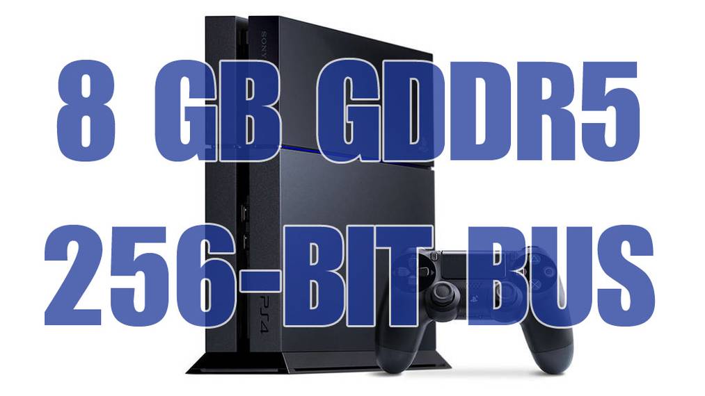
The architecture that we ended up with for PlayStation 4 uses a 256 bit bus and a type of memory found in top-of-the-line graphics cards called GDDR5. The combination of this wide bus and this fast memory gives 176 gigabytes per second [of bandwidth], which -- many of you will have to take my word for it -- is quite a lot.
With that much bandwidth, straightforward programming techniques usually result in some pretty impressive graphics.
Now, we knew that there was an alternative architecture that would be a bit easier to manufacture. In this architecture we would use a narrower 128 bit bus which would drop the bandwidth down to 88 gigabtes per second, which is not particularly good in next generation terms, and therefore would really hurt the graphic performance. So we then used some very fast on-chip memory to bring the performance back up.
If we used eDRAM for this on-chip memory, we knew that bandwidths of as much as one terabyte per second -- that's a thousand gigabytes per second -- would be achievable. The catch though, is that the on-chip memory would need to be very small, and each game team would need to develop special techniques in order to manage it.
To compare these two architectures, the one on the left has 176 gigabytes per second for any access, the one on the right 88 gigabytes per second if the data is in system memory or a thousand gigabytes per second if the data is in that tiny eDRAM. At first glance the architecture on the right looks far superior to the one on the left, and sure, it takes a while to figure out how to use it, but once you understand how to use that little cache of eDRAM, you can unlock the full potential of the hardware.

Surprisingly, especially considering the PS3 precedent (or maybe not surprisingly at all, as Sony learned from its mistakes), the choice didn't fall on the second solution:
But, to our new way of thinking the straightforward approach on the left is definitely advantageous. It gives us excellent day one performance, and we can find other features for the programmers to explore in later years.
In other words, it may be counterintuitive, but 176 is much larger than 1088.
As a result of this "less is more" choice the "time to triangle" (the time necessary to create a graphical system able to match the capabilities of the hardware) has gone back down to the 1-2 months that were necessary for the first PlayStation, from the 6-12 months needed for the PS3, benefitting developers, that already have engines compatible with this PC-like architecture, and indie developers. That terabyte per second of bandwidth may have sounded very tempting, but I bet quite a few devs are now thanking Mark Cerny for deciding against it.